Shin-Etsu Chemical has developed new process technologies, transfer parts and other equipment for Micro LED displays

TOKYO–(BUSINESS WIRE)–Shin-Etsu Chemical Co., Ltd. (Head Office: Tokyo; President: Yasuhiko Saitoh) has developed new process technologies that can be applied for the manufacturing of Micro LED displays.
The size of a Micro LED chip is not visible to the naked eye, with the length of one side being less than 50 μm (micrometers). For example, in order to manufacture one 4K display that has 4 times the resolution of a conventional high-definition screen, it is necessary to precisely array about 24.90 million chips. In order to implement improvements in the complexity and yield ratio in the processes of Micro LED chip manufacturing and the transfer process of each chip, Shin-Etsu Chemical has been working together with Shin-Etsu Group companies to take advantage of our unique materials technologies. We have proceeded to develop various advanced innovative transfer equipment and transfer parts to solve the key manufacturing challenges of Micro LED display manufacturing.
The new process technologies we are announcing were jointly developed with Dexerials Corporation (Head Office: Shimotsuke City, Tochigi Prefecture, Japan; President: Yoshihisa Shinya) and introduces innovative technology that will transfer singulated anisotropic conductive film (ACF) of Φ80μm or less onto the targeted location by laser equipment. Employing this technology, it becomes possible to transfer the singulated ACF only to the designated plate and mount the Micro LED chip on it and makes the repair process in Micro LED display manufacturing easy to carry out, a matter which had been a large issue up until now.
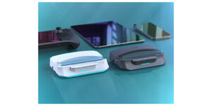
In addition, in order to meet the requests of customers for such matters as achieving further improvements in productivity and in the handling of a wide variety of chips, working in cooperation with two Shin-Etsu Chemical Group companies, Shin-Etsu Engineering Co, Ltd (Head Office: Tokyo; President: Kenji Sugii) and Shin-Etsu Polymer Co., Ltd. (Head Office Tokyo; President: Yoshiaki Ono), Shin-Etsu Chemical developed the following transfer equipment and transfer parts and expanded our products line-up. Combining the advantages of these Shin-Etsu transfer equipment and transfer parts, we will be able to offer the most optimized manufacturing processes to our customers:
SQDP-B Series, cure type donor plate
EZ-PETAMP Series, multi-stage dot-type large stamp (6 inch)
Invisi LUM-X4, a 4-in-1 system that makes it possible to perform 4 processes using 1 laser
BM encapsulant film for Mini LED displays
(For details, please refer to the attached reference material.)
Shin-Etsu Chemical, as a “One-stop Solution Provider” in Micro LED manufacturing, will propose to customers’ solutions to the key challenges presented in the manufacturing processes for Micro LED displays, and we will work to spread the popularity of next-generation Micro LED displays and to expand its position in the display market.
Reference Material
1. SQDP (Shin-Etsu Quartz Donor Plate) —B Series, curing type donor plate
We developed the SQDP-B Series of curing type donor plate that makes laser lift off of Micro LED chips with a solder bump possible. By heat curing after the LED wafer is bonded, it can prevent tilting and cracking of the chips. With this curing type donor plate, laser lift off became possible for Mini LED chips on which cracks can easily have occur and for InGaN (Indium Gallium Nitride) and quaternary system red color Micro LED chips.
2. EZ-PETAMP multi-stage pattern dot-type large stamp (6 inch)
In this way, because there is no interference around the periphery of the chips, it becomes possible to greatly narrow the spacing of the extraordinarily large volume of chips that are being relocated on the second donor plate — much narrower than the pixel pitch. At the same time, by using this product, selective pick up of the chips becomes easy and a remarkable improvement in throughput as well as a reduction of the second donor plate usage volume can be realized.
3. Invisi LUM-X4, a 4-in 1 system that can handle 4 processes with one laser
Shin-Etsu Engineering will market a compact system that integrates the 4 processes that use a laser into one: multi laser lift off, laser mass transfer and high-speed trimming/repair. Unlike the existing system for mass production, not only can all laser processes, from chip singulation to mass transfer and trimming and repair, now be performed using only one laser unit, but also small-quantity production becomes feasible.
4. BM encapsulant film for Mini LED displays
With the technology which Shin-Etsu Chemical has developed of efficiently debonding the support substrate without forming tether, going forward, it is expected that Mini LED chips also will rapidly become thinner as a result of the eliminating of the sapphire support substrate.
Shin-Etsu Polymer, a Shin-Etsu Group company, has developed a film-type black matrix (BM) encapsulant film for Mini LED display applications and it is going forward with customers’ sample evaluations.
This material, in addition to improving the Mini LED display’s contrast, it also performs the function of protecting Mini LED component parts from damage or unclean substances.
Contacts
For inquires about this matter, please contact:Shin-Etsu Chemical Co., Ltd.
Public Relations Dept.
Tetsuya Koishikawa
Tel: 03-6812-2340, or from outside Japan: 81-3-6812-2340
Fax: 03-6812-2341, or from outside Japan: 81-3-6812-2341
e-mail: sec-pr@shinetsu.jpwww.shinetsu.co.jp


